




In the highly demanding world of semiconductor production,every component must meet extreme standards of purity,precision,and stability.One material that has become increasingly important in this industry is PEEK Material(polyether ether ketone).Known for its exceptional mechanical strength and chemical resistance,PEEK plays a critical role in ensuring the reliability of modern semiconductor manufacturing equipment.
A key reason PEEK Plastic is widely used in cleanroom and wafer processing environments is its outstanding resistance to high temperatures.Semiconductor processes often involve thermal cycling,plasma exposure,and aggressive chemicals.Unlike many traditional plastics,high performance Polymer PEEK maintains dimensional stability and mechanical integrity even under continuous stress,making it ideal for precision equipment parts.
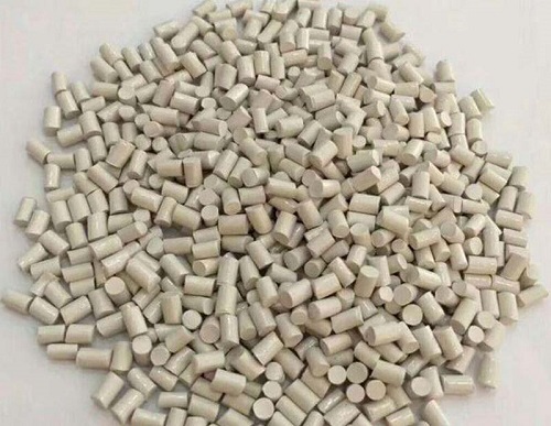
Another important advantage is its excellent chemical resistance.In semiconductor fabrication,equipment is frequently exposed to acids,solvents,and ultra-pure water systems.Engineering thermoplastic PEEK does not easily degrade or contaminate these processes,which is essential for maintaining wafer quality and preventing microscopic defects that could impact chip performance.
In addition,CNC machined PEEK parts are widely used because they can be produced with extremely tight tolerances.Semiconductor tools such as wafer carriers,valve components,insulation parts,and pump systems require high precision to ensure stable operation.PEEK’s machinability allows engineers to create complex geometries while maintaining structural reliability.
Another critical factor is low particle generation.In cleanroom environments,even microscopic contamination can lead to product failure.High purity PEEK material is naturally resistant to particle shedding,making it suitable for ultra-clean semiconductor environments such as photolithography,etching,and deposition systems.
The rise of advanced chip manufacturing has also increased demand for high temperature plastic PEEK components in automated systems.These components are used in robotic arms,wafer handling systems,and precision positioning devices where stability and wear resistance are essential for continuous production.
Today,PEEK material is widely used in:
Wafer processing equipment
Semiconductor chemical delivery systems
Vacuum pumps and sealing components
Photolithography and etching systems
Cleanroom automation equipment
High precision robotic handling systems
As semiconductor technology continues to advance toward smaller nodes and higher precision,manufacturers are increasingly relying on advanced engineering thermoplastics like PEEK to meet strict performance and contamination control requirements.
Key Advantages of PEEK in Semiconductor Equipment
Excellent heat resistance for high-temperature processes
Superior chemical resistance in aggressive environments
High mechanical strength and dimensional stability
Low particle generation for cleanroom compatibility
Suitable for precision CNC machining applications
Long-term reliability in critical equipment systems
FAQ
Why is PEEK material used in semiconductor manufacturing?
Because it offers high purity,excellent chemical resistance,and stability under extreme processing conditions.
Is PEEK suitable for cleanroom environments?
Yes,PEEK has very low particle emission,making it ideal for cleanroom and wafer processing applications.
Can PEEK withstand high temperatures in semiconductor equipment?
Yes,PEEK maintains performance even at continuous high temperatures commonly found in semiconductor processes.
What parts are made from PEEK in semiconductor tools?
Common parts include wafer carriers,seals,insulators,valves,and robotic components.
Why is CNC machining important for PEEK parts?
CNC machining allows high precision and tight tolerances required for semiconductor manufacturing equipment.
